Showing posts with label System 16A. Show all posts

Monday, 13 April 2020

Deconstructing Sega's System 16 Security - Part 2


Sega's FD1089 security module reverse engineering

The FD1089 module variants from Hitachi / SEGA were fabricated in a plastic case, on the back of the module a epoxy layer is visible together with two rows of pins arranged as DIP64. This arrangement mimics a standard 68000 CPU as intended by SEGA.

The sample shown below features the SEGA code 317-0013, this indicates the module was used as the  CPU in Enduro Racer.


As is, the module measures 8.72cm by 2.85cm, not a small piece for a cpu.


The plastic case features a top cover providing access to the battery container, as shown below as many as three batteries could be fitted at once, perhaps allowing for longer data retention configurations. All modules I've seen myself just make use of one battery slot only.

Hitachi seemed to keep most things home by employing Hitachi Maxell CR-2032 3 volt batteries, this one was dated 1986 week 06, that is long enough!

For some reason a white looking dust was found inside all over the battery container, perhaps a battery byproduct over the years?

Lastly, there's a big letter B stamped inside, this corresponds with the specific module type under review: FD1089B. Modules A stamped inside correspond to FD1089A variants.


Time to wear our x-ray glasses so we can see what it looks like inside the module, this is usually one of the most fun parts of a project. For the first time you have a look inside and start making sense of the internals, this one is busy inside and is no standard IC on a package. It's time to start planning an attack.


Easy options first, in order to try gain clean access inside we test the epoxy with a strong paint remover for a couple of days.


Unfortunately this didn't produce any significant results, the epoxy in the FD1089 seems to be well formulated and is resistant to this type of attack.

One step forward, by employing a combination of heat and patience it is possible to separate the plastic case from the epoxy block.


A weak spot on the epoxy curing caused by trapped air is discovered, this allowed for a unique early view of the shinny internal pcb as shown below. 


Time to keep going deeper and figure out how to attack the epoxy, first we take a few extra measurements to understand dimensions, we will need them later on. The epoxy block on its own does 8.49cm by 2.60cm.


With the help of higher resolution x-rays we start to get full control of what's going on in there, eg enumeration and type of devices, guessing the purpose of each device, producing early diagrams, etc...

As shown below, the FD1089 uses a total of four different chips in its operation, left to right: A custom IC (this is where the security magic happens), a 68000 CPU, a 6264 SRAM chip, and a MB3771 voltage monitor (when needed, this takes care of switching power from VCC to VBATT and vice-versa). 

The first three chips are HITACHI bare dies directly glued onto the top of the pcb, the MB3771 is in full form as a surface mounted device soldered to the back of the pcb. 


Next, we need to have a fully validated understanding of the internal interconnect (aka, how things connect to each other and the outside)

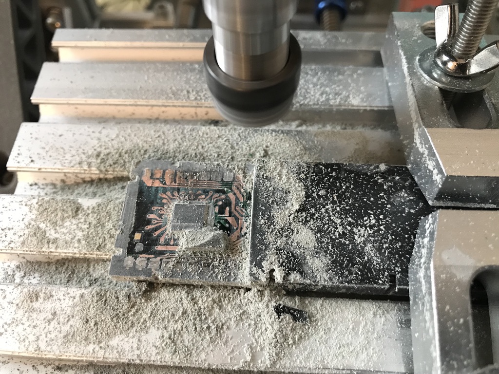
The tool of preference for this project was a precision CNC, nothing fancy, just a standard 1610 model kit from Aliexpress. The goal here is precise enough milling so we reveal the circuit while avoiding fatal damage to the interconnect and chips, especially the custom IC.


Hours later, a significant part of the the copper surface is fully exposed and the custom IC preserved in place, though this didn't come without surprises and a couple of drill bits broken in the process. The reason: just below the IC you can see another unexposed rectangle area, this happened to be a ceramic insert placed there during fabrication to protect access to a sensitive area of the module


At this point a further donor module got dremel down bare in order to understand how many more ceramic inserts were there, in total the FD1089 module has four ceramic inserts, two on the front and two on the back shown below in white, they protect key SRAM signals such as the data bus to prevent extraction of the encryption key through direct drilling.

By now I was convinced these modules were probably very expensive to produce back in the day.


For illustration purposes lets take the following example shown below: Four data bit vias from the SRAM are covered with ceramic, both at the origin near the SRAM as well as at the destination close to the custom IC.

Beyond being cool and almost a hand craft, I'm not sure why this was done, if an attacker could drill from above with the intention of making contact, it could do so at other part of the circuit by exposing the copper, you don't require a via specifically for that.

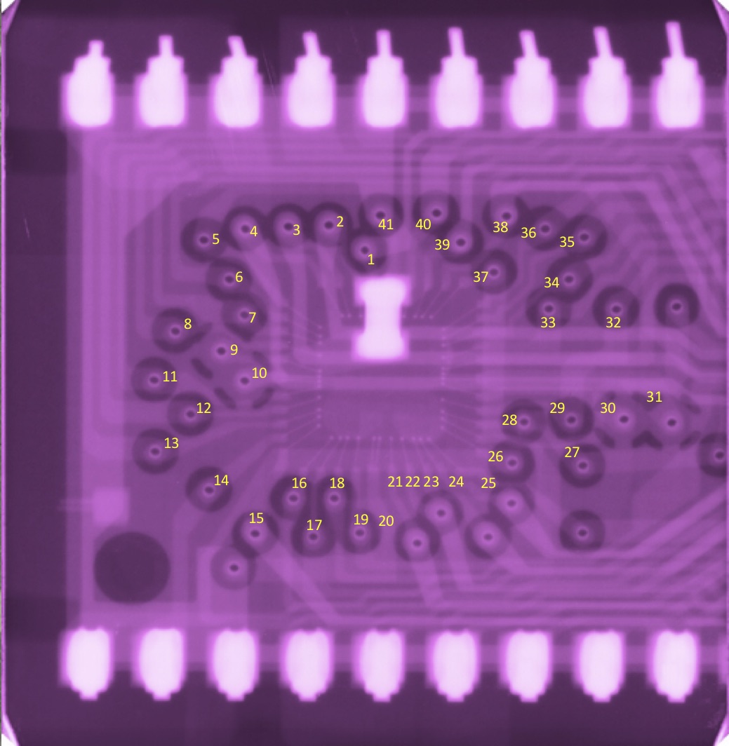


More hours of careful drilling allow us to gain access to further key areas of the pcb, when this process is fully completed it will allow us to work on the next part of the reverse engineering.


Diagraming the interconnect and how chips relate to each other is a critical step before we proceed to examine any deep down chip logic.


Once we are ready to explore the custom chip logic, a further donor unit is put under the knife, the goal here is to cut down the minimum possible sample to allow extraction of the custom IC die housed inside.


Bonus: a cross section of the pcb reveals its four layers, the inner two are dedicated to VCC / GND distribution only.


The smallest possible bite size sandwich is produced, inside not visible is the custom IC, on the left you can see a couple of the white ceramic inserts guarding access.


The sample was then put in a nitric acid beauty spa for several rounds.


At each round the sample was inspected for progress and cleaning. IC dies are very fragile so patience is key, this one waited 30+ years, so it may as well wait another day if necessary. 


Finally getting closer, both ceramic bits are released, we can already see the back of the IC die now exposed.


A final round allowed for the chip die to be fully exposed clean. Pharaonic honors please.


Stay tuned for the next article, we will explore this chip under the microscope. Happy reversing.


Saturday, 12 October 2019

Deconstructing Sega's System 16 Security - Part 1


Sega's System 16 was a new arcade platform introduced in 1986 as a successor to the earlier 8 bit Z80 designs Sega System 1 and System 2. The new system brought in many system upgrades including 16 bit Motorola 68000 CPUs and pioneering security.

Above all System 16 was one of Sega's most successful games platform seeing the release of countless epic games that form part of our collective childhood memories. Among my favorites titles are Shinobi, Golden Axe, Outrun, or Michael Jackson's Moonwalker to name a few, I bet you have yours too.

The platform got subsequent updates and revisions introducing improvements to base specs and integration of chips. The initial System 16A was released in 1986 followed soon by the more common System 16B in 1987, a later revision known as System 18 was introduced in 1989. Specs for all three revisions are as follows:


System 16A specifications

Main CPU: Motorola 68000 or Hitachi FD1089/FD1094 security modules @ 10 MHz
Memory: 16kB + 2 kB
Sound CPU: NEC uPD780C-1 (Zilog Z80) @ 4 MHz
FM synthesis sound chip: Yamaha YM2151 @ 4 MHz (8 FM synthesis channels)
PCM sound chip: NEC uPD7751@ 6 MHz
ADPCM channels: 3
Audio bit depth: 8-bit
Custom GPU chipset: 315-5011 sprite line comparator, 315-5012 sprite generator, 2× 315-5049 tilemap chips, 315-5107 & 315-5108 display timers, 315-5143 & 315-5144 sprite chips, 315-5149 video mixer
Performance: 12.5874 MHz sprite line buffer render clock, 6.2937 MHz sprite line buffer scan/erase & pixel clock
Display resolution: 320×224 to 342×262 (horizontal), 224×320 to 262×342 (vertical), progressive scan
Color palette: 98,304
Colors on screen: 4096 (unique colors) to 6144 (with shadow & highlight)
Graphical planes and sprite capabilities: 2 tile layers (row & column scrolling, 8×8 tiles), 1 text layer, 1 sprite layer. Dual line buffers, double buffering, 128 on-screen sprites, 800 sprite pixels (800.75 sprite processing ticks) per scanline, 100 sprites per scanline, 16 colors per sprite, 8 to 256 width, 8 to 256 height

Fantasy Zone System 16(A) motherboard

Note: a few of the initial System 16 games were released in what's know as Pre-System 16 hardware, this rare system looks pretty much like modified a System1 / 2 pcb.

Alien Syndrome. Pre-System 16 motherboard

System 16B specifications

Sound upgrades
Sound CPU: Zilog Z80 @ 5 MHz or NEC MC-8123 security module
PCM sound chip: NEC uPD7759 ADPCM Decoder @ 640 kHz
ADPCM channels: 8
Audio bit depth: 9-bit
Other features: 8 kHz sampling rate, up to 128 KB audio ROM and 256 samples

Video upgrades
GPU chipset: 315-5196 sprite generator, 315-5197 tilemap generator, 315-5213 sprite chip, 315-5248 & 315-5250 math chips
Sprite capabilities: Sprite-scaling

Wonder Boy III Monster Lair. System 16(B) motherboard

System 18 specifications

Sound upgrades
Sound CPU: Zilog Z80 @ 8 MHz
Sound chip: 2 × Yamaha YM3438 @ 8 MHz + Ricoh RF5c68 @ 10 MHz (8-channel PCM chip, remarked as Sega Custom 315)

Video upgrades
Graphics chips: Sega System 16B chipset, Yamaha YM7101 VDP
Colors on screen: 4096 (unique colors) to 8384 (with shadow & highlight)
Graphical planes and sprite capabilities: 4 tile layers, 1 text layer, 1 sprite layer with hardware sprite zooming, translucent shadows, sprites of any height and length.

Michael Jackson's Moonwalker. System 18 motherboard


Sega meets Hitachi

With the introduction of System 16, selected games replaced the main system 68000 CPU with secretive Hitachi branded device modules, these modules were Hitachi FD1089 revisions A and B, and a more commonly found Hitachi FD1094.


Pictured a couple of HITACHI modules used in Sega System 16 game boards


Most modules feature a sticker with a seven-digit code unique per game title and region. For arcade operators or collectors trying to replace these modules with a regular 68000 CPU or a different Hitachi module, this would result in a non-working game. A battery inside also plays a fatal role, losing its power renders the module unusable.

In combination with encrypted roms the modules provided Sega with a way to control piracy and stop unauthorized board conversions (when a game base system is reused for a different game).

Sega's work with Hitachi was no coincidence, at the time probably no other company in Japan would have the expertise, technology, and rights to be able to produce custom 68000 based modules. Early on Hitachi helped Motorola, the company behind the 68000 CPU, overcome critical manufacturing challenges and achieve repeatable production of the new CPU. In exchange Hitachi was allowed to second source 68000 CPUs under the Hitachi brand.

Hitachi's work with customer modules was not limited to Sega game systems, different modules for different customers were also produced over the years. Here's a few examples found on the net:

FD1095 a custom module close numbered to Sega's FD1094, its purpose or nature is unknown


Several HITACH FD modules found online

Some of these modules can be bought online at present time, in fact, IC supplier Kynix has an active listing selling Sega's FD1094 stock, to verify the validity of the listing I purchased a lot which turned to be right. The modules seem to be refurbished as some of them still contain valid game data and are visibly used.

FD1094 modules purchased from Kynix

Inside the modules

Over the next posts we will discuss the internals of the FD1089 and FD1094 modules, reveal their construction and facts of interest.

Stay tuned.