Tuesday, 11 December 2018

Capcom CPS1 B21 chips in the wild

Do you own any Capcom CPS1 games with a dead or faulty graphics chip? UTsource is holding onto a large new original stock of B21 chips aka DL-0921. According to the listing the stock is at least 86000 units, enough supply for several lifetimes I guess.

To validate the listing I bought a couple of samples and the thing seems definitely real.

NOS Capcom B21 chips as purchased from UTsource.

Saturday, 8 December 2018

Sega System 16 / 18 / 24 / X Security Programming Guide

Dear all, after some lengthy testing we are happy to release full details on the security programing of the Hitachi FD1089 / FD1094 cpus used in Sega's System 16 / 18 / 24 / X motherboards.
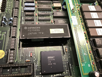

This guide is the result of several years of work by a small group of arcade enthusiasts to unravel the secrets of the security implementation found in one of the most loved and popular arcade game platforms. Thanks to this work it is now possible to fully preserve most Sega 16 bit systems enabled with security as fully working unmodified originals.

Unlike previous projects this time we recommend the usage of a dedicated pcb to interface with the chips due to the high pin count involved in the programming.

Additional details of the inner workings of Sega's FD security modules will be published over time in this blog. Work on the earlier MC 8 bit modules used in some System 1 / 2 boards and sound of Sega 16 is still in progress and will be published when completed. 

Thanks to everyone who has helped make this a reality including all kind donors and testers.

Sega Hitachi FD1089 / FD1094 Security Programming Guide

This document will guide you through the basics of preparing your setup and testing the a clean desuicide method on any known Sega 16 / 18 / 24 / X board revisions using Hitachi FD1089 or FD1094 modules. You can find a pdf copy of this guide and code on the following link: https://github.com/ArcadeHacker/ArcadeHacker_Sega_Hitachi


What's needed


Arduino programmer hardware


  • Soldering iron and solder

Sofrware


Assembling and preparing your Arduino programmer


This step is pretty straight forward, solder all the pin headers to your programmer pcb as well as the IC 64pin socket. The fully assembled pcb looks like this:


After the pcb shield is ready just sandwich it together with your Arduino Mega 2650.


Download and install software for your OS from https://www.arduino.cc/en/Main/Software
Select the right arduino board type before connecting your arduino to your computer. Tools -> Board -> Mega 2560.


Connect the Arduino to your computer by plugin the USB cable and choose the correct serial port in Tools -> Port. 

Open the ArcadeHacker Sega FD1094 or FD1089 .ino file in the Arduino environment. Compile and Upload the sketch to the Arduino unit.

Open the Arduino IDE serial monitor found in Tools -> Serial Monitor. Configure the two settings found in the lower right part of the serial monitor window as follows: Carriage Return and 115200 bauds. 


Close and open the serial monitor, you should now see the following text on screen. If this is the case you have successfully setup and configured your Arduino programmer. 


Programming security keys


Look inside the Arduino FD1089 or FD1094 code for the game you intend to program the encryption keys into the FD chip and uncomment the desired line of code. Only one game can be uncommented at any time, don't forget to comment the default blank game setting at the beginning of the list.


If the above was done correctly you should now compile and upload the program to your Arduino without problems. Once the upload process is finished open the serial monitor found in Tools. The program prompt should display the game you have configured. 


For this example we have selected "eswat" a System 16 game using the Hitachi FD1094 security module "317-0160". FD1094 security modules can be repurposed for any game and it is not required that a label in the cpu module matches the intended game security key to be programmed. This will not be the case with FD1089 modules as two different encryption schemes exist (FD1089A & FD1089B): A variants of the chip are only compatible with games roms for other A variants, and B variants for B games only.


Having inserted the module in the socket we can proceed to program the security keys by typing w and pressing enter. Make sure you replace the module battery if necessary before attempting a key load, a new battery will last at least 20-30 years so don't expect to have to repeat this often. Once the process finishes you can disconnect the Arduino module from your computer and remove the cpu module.


If you would like to verify that the contents of the cpu match the intended configuration loaded in your programmer you can perform a verification by typing v and pressing enter. This verification compares a 1 bit parity per byte calculated internally by the security module against the encryption configuration in your Arduino. 

WARNING: This verification procedure is 100% safe in FD1094 modules. Unfortunately this is not the case with FD1089 modules as the verification will delete the data inside your module, please do not attempt verification with any valuable FD1089 modules especially if currently undumped or not preserved in Mame. 


Final words


This is all there is to preserving your Sega FD1089 / FD1094 modules as working units, we hope this milestone will help you and the rest of the arcade community preserve your loved games as originals and stop the general discarding of Sega Hitachi modules. 

As mentioned in the opening of this post, a number of follow up articles in this blog will reveal the inner workings and curiosities of these artfully crafted security modules. 

Happy preservation. 

Tuesday, 5 June 2018

Sega System 16 Security Reverse Engineering


Dear all,

I'm glad to announce the successful reverse engineering of Sega's System 16 cpu security modules. This development will enable collectors worldwide preserving hardware unmodified, and stop the general discarding of Hitachi FD modules.

The project is right now involving external testers so expect further details and full disclosure over the coming weeks.

Eduardo.

Project credits: Eduardo Cruz, Rockman (Pere ViciƩn), Digshadow, with support from Shinichiro Baba, Ricardo Fernandez-Vega, Andrew Welburn and other kind donators.


Wednesday, 30 May 2018

A Journey Into Capcom's CPS2 Silicon - Part 3

Welcome to the third and last post in the Capcom CPS-2 reverse engineering series, if you missed any of the previous post you can find them here:


Hunting Capcom's Secrets

For many years, finding how and where did Capcom hid away its security implementation has been a pending critical task for the arcade community. CPS2 systems running out of battery were rendered useless forcing collectors worldwide to perform board conversions or let go of their favorite games. 


Typical CPS2 3.6 volts battery made by Hitachi Maxell Ltd in Japan

The battery featured in CPS2 systems is found on the top B board, and it powers a grid that reaches all of the B board customs chips while the board is at rest. During normal operation battery drain is stopped and regular voltage is supplied.

Thanks to Capcom's friendly implementation, battery replacing is a relative safe operation as one is able to switch such battery without fearing instant game death. A capacitor found next to the battery is able to keep things running for a good few minutes until a fresh replacement is soldered. 


Battery voltage measured before distribution to one of the CPS2 custom chips

This grid and the fact Capcom pushes battery power to all custom chips in the board is a deliberate smoke and mirrors exercise in an attempt to deter any curious parties by multiplying the number of possible target chips. 

Earlier security implementations by Capcom such as Kabuki or CPS1 lack this grid scheme and just feature a direct correspondence between the battery and security chip target using it. 


Pulling the string

A clue as to where CPS2 systems hid security came with the introduction of B board revision 5 (93646B-5), from this revision on a little JST NH 6 pin connector was added featuring a number of known and unknown pcb signals. 

Previous to board revision 5 these signals have been found to exist at one of the large base connectors, more specifically base connector CN2.


CN9 as found in CPS2 B board revisions 5 and up


CN2 base connector at a CPS2 B board revion 4

Why would Capcom move these signals into an simpler and more readily accesible connector? If you think in terms of producing, distributing and maintaining tens of thousands of game boards, the move speaks loud of operational and logistics convenience.  Ever scalable, simpler and less expensive processes is a top of mind item for past and present organizations worldwide.

Still a relevant question remained over time: What was behind connector CN9? No game or board feature was known to make any use of it, even worst, any adventurous individuals messing around would quickly find out that playing with this connector ended up mysteriously killing the game. A clear indication about this connector being somehow related to the security implementation of the CPS2 system.


Behind CN9

A quick analysis of CN9 revealed the following findings:


Looking at the list above, pins 1, 5 & 6 carry well known signals involved in the most basic life elements of a game pcb: VCC & GND (Power), and /Reset. Without these it is materially impossible for a game to operate, therefore very relevant signals. 

The remaining pins 2, 3 & 4 don't seem to be driven as no signal is present during operation, most likely inputs with their purpose being unknown. Following the traces for these pins we quickly find them leading onto the adjacent custom chip DL-1827, and no where else. 

Eureka? Time to find out what's behind this IC.

CN9 pins 2, 3, & 4 interface with DL-1827 pins 131, 132 and 69


Inside Capcom's DL-1827

Microscope inspection of DL-1827 revealed a made to order gate array chip manufactured by Fujitsu, more specifically a CG24 series gate array model 692 built on a 0.8 micron CMOS process technology. More information on these chips and gate array technology available on the previous series post. 


Manufacturer marks inside Capcom DL-1827 

Further inspection of the chip logic revealed a shocking finding: DL-1827 is a mere middle-man making no use of such signals. In essence the chip verifies that the board is powered up and drives a passthrough for connector CN9 signals #2, #3 & #4 among several other. The target of such signals entering and exiting DL-1827 is revealed to be the adjacent chip DL-1525.


DL-1827 acts as a passthrough of CN9 signals onto chip DL-1525

The following chart below summarizes how CN9 signals travel until reaching out its destination at chip DL-1525. The analysis discovered that Capcom intentionally used chip DL-1827 to hide away the real security target in CPS2 systems.


CN9 signal journey summary


Inside Capcom's DL-1525

As discussed in the previous post, DL-1525 hosts inside a massive die measuring around 7x7mm in size featuring a majestic Motorola 68000 megacell core surrounded by a vast 3-layer gate array. Inside of this sea of gates one area in particular hosts a large section of memory registers used to store some configuration settings and the game encryption keys. 

A total of 158 bits (1 bit per memory register) are chained together in a serial train to compose the memory block used as part of these settings found in CPS2 security.


DL-1525 Motorola H4C057 class gate array, memory dedicated array area highlighted.

A closer look of the area shows the structures identified as memory registers.

Group of gate array memory registers highlighted in purple and green.

Below, verification of such structures in the simulator reveals the memory registers as D type flip-flops. Top right of the image: 20x chip gate array area capture of a flip-flop memory register.
Top left and bottom images: logic simulation for verification purposes.

CPS2 DL-1525 gate array D type flip flop overview and simulation

Example of how one of the CN9 signals enters the DL-1525 chip: Bottom left in yellow CN9 #3 enters DL-1525 through pin 9 and is driven through a buffer for signal amplification purposes. After that the signal goes straight into the first memory register enable input, then connected to the rest of registers as a series of chains.


Overview of CN9 #3 signal entering DL-1525 through pin 9


Structure of the memory

The 158 bits used in CPS2 security configurations are structured in 4 differentiated blocks. One of them is dedicated to configuration settings while another three contain specific encryption information such as the pair of encryption keys.

From the outside configurations are stored in the chip via serial a protocol in bit reverse order, while the system inside access the information in full parallel mode (all bits at once).

Example CPS2 internal configuration for the game sfz2alh 

As displayed above a number of bits in the first block are of unknown purpose, from here i'd like to invite any brave readers to venture in finding their exact use and functionality.

All information regarding how to write CPS2 security configurations can be found here.


Closing words

Working on unraveling the mysteries behind the CPS2 security implementation has been an amazing challenge and journey for me. I'd like to thank every person that has participated, helped or backed the project in any way, specially to those deeply involved: Artemio Urbina, Ian Court and Digshadow.

The arcade legacy still has a great number of preservation challenges waiting to be addressed that will keep us entertained for while. I look forward to share new and exciting projects with you in the near future.

Eduardo.

Sunday, 4 March 2018

Is Your Gaming CRT Exposing You to X-Rays?

Motivated by this discussion at UKVAC I decided to run a little experiment to find out if your typical gaming CRT leaks any measurable X-rays. Tan while having fun? Let's find out.

Test Setup 

My setup involved testing three tubes in my collection used from time to time for testing arcade pcbs, retro consoles, as well as micro computers. I believe these models are also commonly found among the gaming community and they should be somehow representative.

In front of each tube an X-ray sensor is placed at different distances: 3cm, 30cm, 60cm. X-ray activity is sampled during 180 seconds during each run, then compared against ambient readings (tube turned off).

Initially the X-ray sensor is left to warm up for a good 10 minutes to obtain constant ambient reads.

NEC XM29

Sony BVM-20F1E

Toshiba A68 CRT (NANAO MS9) on a New Astro City cab

The Results

I'm afraid to break the news but... there's no such thing as a free tan while retro gaming. At no time any of the tubes tested presented any abnormal sensor reads indicating the presence of X-rays. To put things into perspective I have included a table below comparing the different scenarios together with reads of the sensor exposed to radiation from a controlled x-ray source.


I'm no expert on this matter, but even if the energies inside the tube are high enough to produce X-rays, the glass in your CRT has lead in it to block those from reaching you. Perhaps someone with enough expertise could confirm these assumptions.

Happy safe gaming.

Tuesday, 2 January 2018

A Journey Into Capcom's CPS2 Silicon - Part 2

Welcome to the second post in the Capcom CPS-2 reverse engineering series, if you missed the previous post you can find it here:


Inside the custom chips of CPS2


Capcom's Play System 2, also known as CPS2, was a new arcade platform introduced in 1993 and a firm call on bootlegging. Featuring similar but improved specs to its predecessor CPS1, the system introduced a new security architecture that gave Capcom for the first time a piracy-free platform. A fact that remained true for its main commercial lifespan and that even prevented projects like Mame from gaining proper emulation of the system for years.


Chip Makers

Capcom's extensive use of customs in CPS2 spreads over a total 11 QFP type chips, as part of this project each of the chips were decapped and identified as follows:

A board (Base board)

DL-0311: Ricoh A5C series, standard cells. (Also found in CPS1) Datasheet
DL-0921: Ricoh A5C series, standard cells. (Also found in CPS1) Datasheet
DL-1123: Hitachi HG62F series model 22, gate array. Datasheet
DL-1425: AT&T Digital Signal Processor WEDSP16A-M14. (Also found in CPS1.5) Datasheet
DL-1625: VLSI Technology (VTI) VGT300 series model 022, gate array. Datasheet
DL-2227: Hitachi HG62E series model 08, gate array. Datasheet

CPS2 A Board 93646A-3 Custom chips highlighted


B board (Top board)

DL-1525: Motorola H4C series model 057, gate array in combination with a 68000 cpu megacell (CPM68K REV7-89). Datasheet
DL-1727: Fujitsu CG24 series model 692, gate array. *
DL-1827: Fujitsu CG24 series model 692, gate array. *
DL-1927: Fujitsu CG24 series model 512, gate array. *
DL-2027: Fujitsu CG24 series model 512, gate array. *

* No datasheet available for the Fujitsu CG24 series, please share any.

CPS2 B Board 93646B-6 Custom chips highlighted


Gate Array technology

Used in most CPS2 custom chips, a gate array circuit is a prefabricated silicon chip circuit with no defined functionality, in which transistors, standard NAND or NOR logic gates, are placed following a regular pattern and manufactured on a wafer, this half baked wafer is known as master slice.

Common advantages of Gate Arrays designs over Full-Customs according to TU Delft:

Minimization of the fabrication time: Because the chips are prefabricated (the transistors are already on the master image), the silicon foundry only processes the masks related to metal wires. As compared to full custom layout, the number of masks processed by the silicon foundry is often reduced by more than 60%.

Minimization of the design time: The time involved in designing a cell layout is reduced dramatically (as compared to full-custom) because the transistors are pre placed on the image. Typically, it takes only a few minutes to layout a flipflop or a combinatorial gate, and the designer does not need to know much about the process design rules.

Minimization of the chip cost: The layout design starts with a prefabricated master image. This is a semi-manufactured article that can be produced in large quantities. Consequently, it can be cheap.


Gate Array die size and development time compassion versus other chip design technologies


The Fujitsu gate array chips featured in CPS2's B board belong to the CG24 series and use a 0.8 micron CMOS process. Fujitsu uses a block-level placement and routing scheme commonly known as "fishbone".


Markings inside CPS2 Gate Array chip DL-2027


Unwired section of NAND sea-of-gates inside a Fujitsu CG24 chip

Logic inverter (NOT) implemented in Fujitsu's NAND sea-of-gates

Fujitsu's gate array technology is discussed in more detail in 1978 USPTO patent 4,412,237: https://docs.google.com/viewer?url=patentimages.storage.googleapis.com/pdfs/US4412237.pdf


Capcom's deep pockets

Interestingly enough, several of the B board's chips used by Capcom show a very low utilization of resources being the worst offender chip DL-2027. In IC density terms its contents could be classified as mostly empty space. 

Given the expensive nature of the end to end design and fabrication of these devices one must think that perhaps Capcom's market successes enabled the company not to spare in resources.


Highlighted in yellow: total die area utilization inside DL-2027 


The Mysterious CPU


Contrary to popular belief, Capcom's CPS-2 cpu does not reside on the A bottom board of the system, instead the cpu is found on the B board and inside the big 208 pin QFP chip labeled as DL-1525. MAME's own documentation on CPS-2 does not help this belief either as it also states the system cpu is DL-1625, an A board chip.


Capcom DL-1525 dated 1993 week 51 source id JSX02RJ524AU03

DL-1525 hosts inside a massive die measuring around 7x7mm in size featuring a majestic Motorola 68000 megacell core surrounded by a vast 3-layer gate array. This monster IC is based on the Motorola H4C gate array series and uses a gate length of 0.7 microns (700 nanometers). To date it is the smallest feature sized chip I have worked on since I began reverse engineering ICs.


DL-1525 is a Motorola H4C057 class gate array in combination with a 68k cpu core (top right)


Small section of DL-1525 captured at 50x magnification. Three routing metal layers are visible.


Cross-section view of a Motorola H4C gate array describing its composition


DL-1525 Ancestry

A newsletter from Dataquest from May 1988 traces back the origins of Motorola's blending of 68000 cores with gate arrays to the world of laser printers. An extract of such IC industry newsletter reads as follows: 
Motorola is designing gate-array-based interface chips for use in laser printers. The chips will contain a core of the 68000 microprocessor and the dedicated laser printer functions. The LPC-1 will have 5,000 gates and will be fabricated with a 2-micron CMOS technology, while the ALPC-1 will have 16,000 gates and will be the first commercial application of Motorola's HDC series of 1-micron CMOS channelless architecture gate arrays. The LPC-1 is currently available in sample quantities; samples of the ALPC-1 will be available in December, with volume production scheduled for February 1989.

In fact, additional research shows chips with similar source identification marks to Capcom's DL-1525 have been in use in commercial laser printers such as models A258/A259/A260 made by Ricoh. The following parts catalog mentions at least two relevant ICs listed as follows:

 JSC05RR519AU15   208QFP // RICOH IPU BOARD A259 5146 / A260 5146
 JSC05SV519AY17   240QFP // Ricoh main control board A258 5090

Another close brother to DL-1525 is Motorola's own MC68302 "Integrated Multiprotocol Processor" chip. This IC employs a similar gate array and embedding of a 68k cpu core inside. More details about it can be found in the following document and product manual.


MC68302 internals description found in "Image Processing For Future High Energy Physics Detectors"

Other chips from Motorola are known to exist with even closer source id numbers to Capcom's DL-1525, their purpose or end product usage are unknown: 

 JSX02RJ514AU17   208QFP // H4C057-68K 
 JSX02RJ524AU03   208QFP // Capcom CPS2 DL-1525
 JSX05PR511AW26  144QFP
 JSX05PR511AW27  No info
 JSX38PG511AJ03   No info


DL-1525 in the wild

Another interesting finding regarding DL-1525 was the availability of chip stock in Alibaba.com marketplace, during March of 2017 and to test the listing veracity I was able to successfully purchase brand new stock of JSX02RJ524AU03 from a Chinese reseller. At the time of writing of this blog post such stock seems to be still listed on sale online. This chip doesn't seem to be the only Capcom device being sold in the wild, other chip codes are available to purchase online. 

I guess this is of no commercial relevance to Capcom anymore, but overall it doesn't show great asset control practices.


Two NOS units of Capcom's DL-1525 chip sourced from China, chips dated 1998 week 24

This is all for now, I hope you have enjoyed Part 2 of the CPS2 reverse engineering series. On the next post we will explore how and where Capcom hided its CPS2 security implementation. Stay tuned.

Part 3